|
Atom-in-PC Hardware  Roland Leurs wrote this page realizing there is much more to say about the hardware but the most important things are mentioned. Take a look at the Dutch manual (220kB) if you have any questions. Last update by R.Leurs: december 12, 1999. Contents: 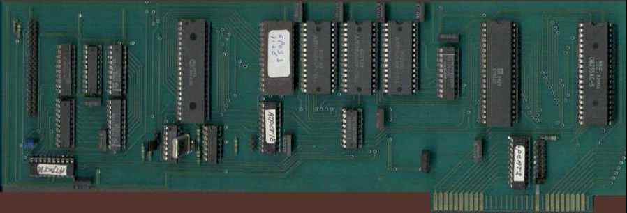 The Atom in PC board (± 34 x 10 cm) Hardware description As in the original Atom, the address space #B000-#BFFF is reserved
for I/O purposes. I used the address space #B000-#B97F for on-board
I/O such as the 6522 VIA, a latch for controlling NMI (see video
emulation), utility RAM select and Video Write Address Latches.
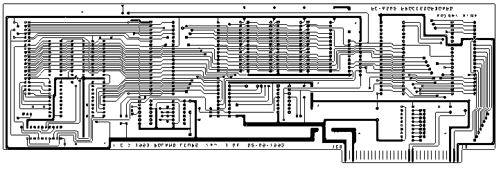
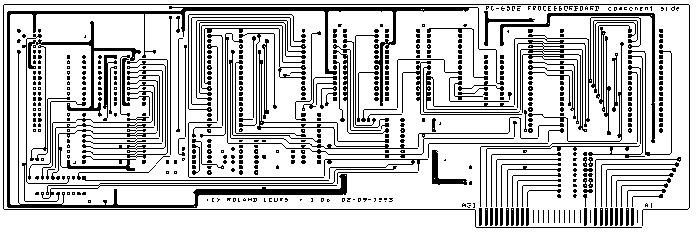
Printed Circuit Board This is the most critical part if you start building your own Atom-in-PC board. You have to download the design, make a good hardcopy of it and make a printed circuit board. Let's take a look at the design: (click on it for a more detailed picture) 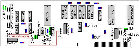 Print layout (there is a 'silk screen' picture in the zip file)
You can download the PCB design in AutoCAD
2.0 DXF format or Epson 132 column PRN format. In the latter, just put a new ribbon in your printer and type copy .prn lpt1 where is one of the files in the zipfile.
GAL Logics
The PC Address decoder GAL is used for selecting the 8255 PPI on the Atom-in-PC board. In this design it decodes eight address spaces of 4 bytes each in the address range 0x300-0x31F. Of cource, you are free to change the algorithm if you need to use another address. You can start the terminal program with an address parameter, so the software is ready for your change!
PC ADRES DECODER-DESIGN GAL16V8A
DATE 08/03/93
BY: R.LEURS
CHIP DECODERP GAL16V8A
NC A2 A3 A4 A5 A6 A7 A8 A9 GND
AEN CS300 CS304 CS308 CS30C CS310 CS314 CS318 CS31C VCC
EQUATIONS
/CS300 = /AEN*A9*A8*/A7*/A6*/A5*/A4*/A3*/A2
/CS304 = /AEN*A9*A8*/A7*/A6*/A5*/A4*/A3*A2
/CS308 = /AEN*A9*A8*/A7*/A6*/A5*/A4*A3*/A2
/CS30C = /AEN*A9*A8*/A7*/A6*/A5*/A4*A3*A2
/CS310 = /AEN*A9*A8*/A7*/A6*/A5*A4*/A3*/A2
/CS314 = /AEN*A9*A8*/A7*/A6*/A5*A4*/A3*A2
/CS318 = /AEN*A9*A8*/A7*/A6*/A5*A4*A3*/A2
/CS31C = /AEN*A9*A8*/A7*/A6*/A5*A4*A3*A2
The second GAL takes care of most of the address decoding within the 6502 memory space. Nice feature (not a bug!): if you pull down pin 9 to 0 volt all on-board memory and I/O devices are disabled. So you can replace all memory and I/O by external circuits without modification of the Atom-in-PC board.
ATOM ADRES DECODER - DESIGN 16V8A
DATE 09/03/93
BY: R.LEURS
CHIP DECODERA_V2 GAL16V8A
A15 A14 A13 A12 RW FI2 WP OSRAM ENABLE GND NC1 CS_IO FI2OUT RWOUT
NWDS CS_PROG CS_UTIL CS_VIDEO CS_ROM VCC
@UES RL09034a
EQUATIONS
 FI2OUT = FI2
/RWOUT = /RW
/NWDS = FI2*/RW
/CS_IO = A15*/A14*A13*A12*ENABLE
/CS_UTIL = A15*/A14*A13*/A12*RW*ENABLE
 + A15*/A14*A13*/A12*/RW*/WP*ENABLE
 CS_PROG = A15+/A15*/A14*/A13*A12*WP*/RW+/ENABLE
/CS_VIDEO = A15*/A14*/A13*ENABLE
 + A15*A14*OSRAM*RW*ENABLE
 + A15*A14*/WP*/RW*ENABLE
/CS_ROM = A15*A14*/OSRAM*RW*ENABLE
The last GAL device takes care of selecting an internal I/O device and generating a NMI signal to the processor if there is a video memory write-cycle going on.
ATOM VIDEOKAART-DESIGN GAL16V8A
DATE 14/1/1995
BY: R.LEURS
CHIP VIDEO GAL16V8A
CS NMI_EN RW O2 A0 A1 A13 A14 A15 GND
IOSEL VIASEL LATSEL DIR NC NRDS LATCH CS_ADL CS_ADH VCC
; IOSEL = SELECTIE I/O GEBIED (DECODER GAL PIN 12)
; VIASEL = SELECTIE VIA (74HCT138 PIN 15)
; LATSEL = SELECTIE LATCH (74HCT138 PIN 14)
; CS = SELECTIE VIDEOGAL (74HCT138 PIN 13)
; DIR = RICHTING DATATRANSPORT (74HCT245 PIN 1)
EQUATIONS
/LATCH = A15 * /A14 * /A13 * /RW * O2 * NMI_EN * IOSEL *
 VIASEL * LATSEL
/CS_ADL = RW * /A1 * /A0 * /CS
/CS_ADH = RW * /A1 * A0 * /CS
/NRDS = RW * O2
 DIR = /RW
If you have your own GAL assembler software you can modify these designs as you like. There is no need to modify the Atom address decoder GAL and the Video & I/O controller GAL. A long time ago, I downloaded PALASM from "http://www.amd.com/support/software.html" AMD website = Maybe it's still available there. Otherwise, if you have no software to assemble the GALs, or the hardware to program the GALs, please send me an e-mail. In the download section of the On this site is a file named gals.zip with the sources en binary files available. Roland Leurs wrote this page realizing there is much more to say about the hardware but the most important things are mentioned. Take a look at the Dutch manual if you have any questions. If reading Dutch is a problem for you then send me an e-mail Last update by R.Leurs: december 12, 1999. Grace to Roland who alowed me to put these pages on my site. Haydn. 
|