| D5 | --> | _1 | SN -76489- -AN- |
16 | <-- | VCC |
| D6 | --> | 2 | 15 | <-- | D4 | |
| D7 | --> | 3 | 14 | <-- | CLOCK | |
| READY | <-- | 4 | 13 | <-- | D3 | |
| !WE | --> | 5 | 12 | <-- | D2 | |
| !CE | --> | 6 | 11 | <-- | D1 | |
| AUDIO OUT | <-- | 7 | 10 | <-- | D0 | |
| GND | --- | 8 | 9 | --- | NC |
NB: Texas Instruments at one time decided to name the most significant bit as bit zero, and increment into the less significant bits. Thus, a byte would be labelled as D0 to D7, instead of D7 to D0 like everyone else. This chip and its data sheet are from that time but this on-line document uses the standard convention to avoid confusion. The figures have been edited too.
This chip has a synthesisable model, written by Arnim Läuger, for his VHDL implementation of the Colecovision. It can be extracted for implementing other machines such as the BBC micro.
* Part SN76489N is identical to the SN76489A except that the maximum clock input frequency is 500 kHz. A "divide by eight" stage is deleted from the input circuitry and only 4 clock pulses are required to load the data, compared to 32 pulses from the SN76489AN.
TEXAS INSTRUMENTS RESERVES THE RIGHT TO MAKE CHANGES AT ANY TIME IN ORDER TO IMPROVE DESIGN AND TO SUPPLY THE BEST PRODUCT POSSIBLE.
The SN76489AN digital complex sound generator is an I2L/Bipolar IC designed to provide low-cost tone/noise generation capability in microprocessor systems. The SN76489AN is a data bus based I/O peripheral.
| Parameter | Min. | Typ. | Max. | Units |
| Supply Voltage, VCC | 4.5 | 5.0 | 5.5 | V |
| High-Level Output Voltage, VOH (pin 4) | 5.5 | V | ||
| High-Level Output Current, IOL (pin 4) | 2 | mA | ||
| Operating Free-Air Temperature, TA | 0 | 70 | °C |
Each tone generator consists of a frequency synthesis section and an attenuation section. The frequency synthesis section requires 10 bits of information (F9-F0) to define half the period of the desired frequency (n). F9 is the most significant bit and F0 is the least significant bit. This information is loaded into a 10 stage tone counter, which is decremented at a N/16 rate where N is the input clock frequency. When the tone counter decrements to zero, a borrow signal is produced. This borrow signal toggles the frequency flip-flop and also reloads the tone counter. Thus, the period of the desired frequency is twice the value of the period register.
The frequency can be calculated by the following:
f = N / 32n
where N = ref clock in Hz
n = 10 bit binary number
The output of the frequency flip-flop feeds into a four stage attenuator. The attenuator values, along with their bit position in the data word, are shown in Table 1. Multiple attenuation control bits may be true simultaneously. Thus, the maximum attenuation is 28 dB.
Table 1: ATTENUATION CONTROL BIT POSITION
| A3...0 | Attenuation weight / dB |
| 0001 | 2 |
| 0010 | 4 |
| 0100 | 8 |
| 1000 | 16 |
| 1111 | Off |
The Noise Generator consists of a noise source and an attenuator. The noise source is a shift register with an exclusive OR feedback network. The feedback network has provisions to protect the shift register from being locked in the zero state.
Table 2: NOISE FEEDBACK CONTROL
| FB | Configuration |
| 0 | "Periodic" Noise |
| 1 | "White" Noise |
Whenever the noise control register is changed, the shift register is cleared. The shift register will shift at one of four rates as determined by the two NF bits. The fixed shift rates are derived from the input clock.
Table 3: NOISE GENERATOR FREQUENCY CONTROL
| NF bits | Shift rate |
| 00 | N/512 |
| 01 | N/1024 |
| 10 | N/2048 |
| 11 | Tone Generator #3 Output |
The output of the noise source is connected to a programmable attenuator as shown in Figure 4.
The output buffer is a conventional operational amplifier summing circuit. It sums the three tone generator outputs, and the noise generator output. The output buffer will generate up to 10 mA.
The microprocessor interfaces with the SN76489AN by means of the 8 data lines and 3 control lines (!WE, !CE and READY). Each tone generator requires 10 bits of information to select the frequency and 4 bits of information to select the attenuation. A frequency update requires a double byte transfer, while an attenuator update requires a single byte transfer.
If no other control registers on the chip are accessed, a tone generator may be rapidly updated by initially sending both bytes of frequency and register data, followed by just the second byte of data for succeeding values. The register address is latched on the chip, so the data will continue going into the same register. This allows the 6 most significant bits to be quickly modified for frequency sweeps.
The SN76489AN has 8 internal registers which are used to control the 3 tone generators and the noise source. During all data transfers to the SN76489AN, the first byte contains a three bit field which determines the destination control register. The register address codes are shown in Table 4.
Table 4: REGISTER ADDRESS FIELD
| R2...0 | Destination control register | |
| 000 | Frequency | Tone 1 |
| 001 | Attenuation | |
| 010 | Frequency | Tone 2 |
| 011 | Attenuation | |
| 100 | Frequency | Tone 3 |
| 101 | Attenuation | |
| 110 | Control | Noise |
| 111 | Attenuation | |
The formats required to transfer data are shown below.
| _7 | _6 | _5 | _4 | _3 | _2 | _1 | _0 | <- Conventional data bus bits (D7=MSB on Left, D0=LSB on Right) |
| 1 | R2 | R1 | R0 | F9 | F8 | F7 | F6 | Update frequency (double byte transfer) |
| 0 | x | F5 | F4 | F3 | F2 | F1 | F0 | |
| 1 | R2 | R1 | R0 | x | FB | NF | Update noise source (single byte transfer) | |
| 1 | R2 | R1 | R0 | A3 | A2 | A1 | A0 | Update attenuator (single byte transfer) |
The microprocessor selects the SN76489AN by asserting !CE (active low). Unless !CE is asserted, no data transfer can occur. When !CE is asserted, the !WE signal strobes the contents of the data bus to the appropriate control register. The data bus contents must be valid at this time.
The SN76489AN requires approximately 32 clock cycles to load the data into the control register. The open-collector READY output is used to synchronize the microprocessor to this transfer and is pulled low immediately following the leading edge of !CE. It is released to be pulled high (by an external pullup resistor) when the data transfer is complete.
The data transfer timing is shown below.
Figure 1. DATA TRANSFER TIMING

Table 5: FUNCTION TABLE*
| Inputs | Output | |
| !CE | !WE | READY |
| 0 | 0 | 0 |
| 0 | 1 | 0 |
| 1 | 0 | 1 |
| 1 | 1 | 1 |
* This table is valid when the device is:
The table below defines the SN76489AN pin assignment and describes the function of each pin.
| Name | Pin | I/O | Function |
| !CE | 6 | In | !Chip Enable – when active (low) date may be transferred from CPU to the SN76489AN. |
| D7 (MSB) | 3 | In | The data bus through which control data are input. |
| D6 | 2 | ||
| D5 | 1 | ||
| D4 | 15 | ||
| D3 | 13 | ||
| D2 | 12 | ||
| D1 | 11 | ||
| D0 (LSB) | 10 | ||
| VCC | 16 | In | Supply Voltage (5V nominal) |
| GND | 8 | Ground Reference | |
| CLOCK | 14 | In | Input Clock |
| !WE | 5 | In | Write Enable – when active (low), !WE indicates that data is available from the CPU to the SN76489AN. |
| READY | 4 | Out | When active (high), READY indicates that the data has
been read. When READY is low, the microprocessor should enter a wait state until READY is high. |
| N.C. | 9 | No external connection should be made in this pin. | |
| AOUT | 7 | Out | Audio Drive Out |
| PARAMETER | TEST CONDITIONS | MIN | TYP | MAX | UNITS | ||
| II | Input Current | VIN = GND to VCC | !CE | -25 | 175 | µA | |
| D0-D7, !WE, CLK | -10 | -10 | |||||
| VOL | Low Level Output Voltage |
IOUT = 2 mA READY | .25 | .4 | V | ||
| ICC | Supply Current | Outputs Open | 30 | 50 | mA | ||
| CI | Input Capacitance | 15 | pF | ||||
| IOH | High Level Output current |
Vcc < 5.0V | 20 | µA | |||
| 5.0V < VCC < 5.5V | 300 | ||||||
| VIH | High Level Input Voltage |
D0-D7, !WE, !CE, CLK | 2 | V | |||
| VIL | Low Level Input Voltage |
.8 | |||||
| 2 dB | Attenuation | 1 | 2 | 3 | dB | ||
| 4 dB | 3 | 4 | 5 | ||||
| 8 dB | 7 | 8 | 9 | ||||
| 16 dB | 15 | 16 | 17 | ||||
Figure 2. EXTERNAL AUDIO INPUT INTERFACE
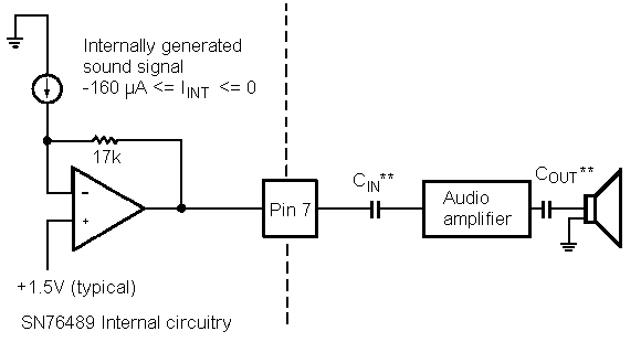
** These capacitance values are determined by the frequency response desired and the audio amplifier used.
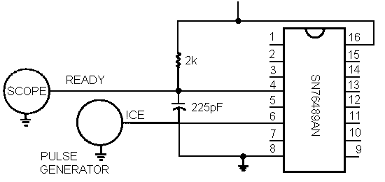
| PARAMETER | TEST CONDITIONS | MIN | TYP | MAX | UNITS | |
| *!CE to READY | CL = 225pF | |||||
| tPLL, 50% to 50% | RL = 2K to VCC | 90 | 150 | ns | ||
| fclock, Input Clock Frequency | Clock Transition Time (10% to 90%) 10 µs | DC | 3.579 | 4 | MHz | |
| Setup Time, tsu (see Figure 1) | DATA w.r.t. !WE | 0 | ns | |||
| !CE w.r.t. !WE | 0 | |||||
| Hold Time, th (see Figure 1) | DATA w.r.t. READY | 0 | ||||
*!CE Pulse: 0-3V, trise <= 7ns, tfall <= 7ns
Figure3. tPLL TEST CIRCUIT

This device consists of three programmable tone generators, a programmable noise generator, a clock scaler, individual generator attenuators and an audio summer output buffer. The SN76489AN has a parallel 8 bit interface through which the microprocessor transfers the data which controls the audio output.
